EasyEDA - Free Schematic & PCB Design + Simulation Software Review
2016-05-18
[public] 295K views, 6.37K likes, dislikes audio only

Thanks to EasyEDA for sponsoring this video
Have a look if you are interested: https://easyeda.com/
Previous video: /youtube/video/QnUhjnbZ0T8
Facebook: https://www.facebook.com/greatscottlab
Twitter: https://twitter.com/GreatScottLab
Support me for more videos: https://www.patreon.com/GreatScott?ty=h
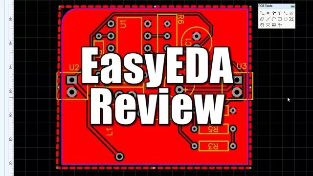
In this video I will create a PCB layout for my ATtiny Boost Converter with the help of the free Software EasyEDA. Along the way I will tell you what I like and don't like about the program.
Music:
2011 Lookalike by Bartlebeats
Killing Time, Kevin MacLeod (incompetech.com)
search for component symbols and packages
/youtube/video/SpKK6o4ffts?t=109.069
/youtube/video/SpKK6o4ffts?t=109.069
convert the schematic into a pcb layout
/youtube/video/SpKK6o4ffts?t=165.23
/youtube/video/SpKK6o4ffts?t=165.23
measuring the distance between two leads of components
/youtube/video/SpKK6o4ffts?t=208.00999
/youtube/video/SpKK6o4ffts?t=208.00999
attach the voltage probe to the input and outputs
/youtube/video/SpKK6o4ffts?t=273.88901
/youtube/video/SpKK6o4ffts?t=273.88901