2020-11-15
[public] 122K views, 11.7K likes, 48.0 dislikes audio only
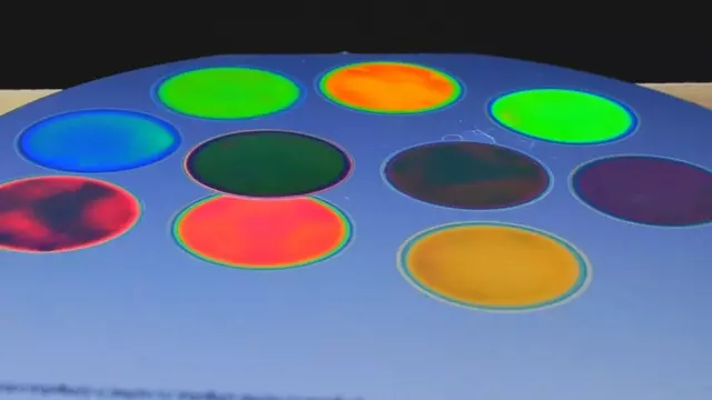
Passing an electrical current through a silicon wafer in a special acid etchant will create a porous layer with a variable index of refraction. I describe how this process works, and how the Fourier transform relates filter design to electrical etch waveform and resulting spectral response.
Notes: 1. The Rugate filters look especially good in polarized light because the reflection from the silicon wafer is reduced, but the reflection from the filter remains strong. I noticed this while holding the wafer in front of my computer monitor. Later, when showing it to friends, the color intensity was poor. Their monitor must have been horizontally polarized, so holding the wafer low, and tilting it upward didn't work! Some monitors are horizontally polarized, and some are vertical.
2. The magnet used to hold down the PTFE cup to the wafer may have a very slight impact on the etch process. The dramatic shift in filter performance at the periphery is due to O-ring restricting the conductive etchant to a sharp edge, creating an electrical field concentration.
Outstanding visual Fourier series tutorial:
http://www.jezzamon.com/fourier/index.html
LR-1 spectrometer: http://www.aseq-instruments.com/LR1.html
p-type wafers on eBay. (You have to hunt around and check the photos for info on the label attached to the box of wafers. Be sure to get wafers less than 0.01 ohm-cm) eg https://www.ebay.com/itm/25-silicon-wafer-P-type-150mm-100-sumco/263441166009 n-type wafers are photosensitive during the etch process.
Online graphing calculator page from this video: https://www.desmos.com/calculator/hiju8zdqfz
Original Desmos page that I used: https://www.desmos.com/calculator/qpnz9celzf
Code for Keithley 2450 control and processing.org waveform generation:
https://github.com/benkrasnow/Porous_Silicon_Optics
Fourier transform to understand optical coatings:
http://www.willeyoptical.com/pdfs/92_180.pdf
Porous silicon refs:
https://www.rp-photonics.com/rugate_filters.html
https://www.intechopen.com/books/porosity-process-technologies-and-applications/porous-silicon
https://sci-hub.se/https://doi.org/10.1016/j.mee.2011.03.143
https://sci-hub.se/https://doi.org/10.1080/10408436.2010.495446
https://sci-hub.se/https://doi.org/10.1007/978-3-319-71381-6_2
https://sci-hub.se/https://doi.org/10.1364/AO.44.005415
https://sci-hub.se/10.1364/OE.16.015531
https://sci-hub.se/https://doi.org/10.1002/adma.19940061214
https://sci-hub.se/https://doi.org/10.1063/1.2906337
Silicon wafer identification flats:
https://www.tf.uni-kiel.de/matwis/amat/elmat_en/kap_5/illustr/i5_2_4.html
Applied Science on Patreon:
https://www.patreon.com/AppliedScience
/youtube/video/iwj78pR46zM?t=0
/youtube/video/iwj78pR46zM?t=40
/youtube/video/iwj78pR46zM?t=205
/youtube/video/iwj78pR46zM?t=249
/youtube/video/iwj78pR46zM?t=408
/youtube/video/iwj78pR46zM?t=568
/youtube/video/iwj78pR46zM?t=798
/youtube/video/iwj78pR46zM?t=893
/youtube/video/iwj78pR46zM?t=975
/youtube/video/iwj78pR46zM?t=1042
/youtube/video/iwj78pR46zM?t=1093
/youtube/video/iwj78pR46zM?t=1117
/youtube/video/iwj78pR46zM?t=1185
/youtube/video/iwj78pR46zM?t=1274
/youtube/video/iwj78pR46zM?t=1307
/youtube/video/iwj78pR46zM?t=1348
/youtube/video/iwj78pR46zM?t=1416
/youtube/video/iwj78pR46zM?t=1524
/youtube/video/iwj78pR46zM?t=1587
/youtube/video/iwj78pR46zM?t=1691

